The semiconductor die inside an integrated circuit is only part of what determines real-world performance. The IC package—the physical structure surrounding the silicon—affects how heat leaves the die, how signals behave, how the device is soldered, how it is inspected, and how reliable it remains in service.
IC package types describe the physical form of an integrated circuit, including how it mounts to the PCB, how its pins or pads connect electrically, and how well it handles heat, assembly, and high-speed signals. Common IC package types include DIP, SOIC, TSSOP, QFN, BGA, WLCSP, QFP, DFN, SOT-23, and TO packages. The best package depends on whether you need easy hand soldering, compact size, strong thermal performance, high-speed signal integrity, or high pin density.
Choosing the right IC package matters in consumer devices, industrial automation, automotive electronics, medical equipment, RF products, and IoT systems. Datasheets list the electrical specs, but the package often determines whether the part will be practical to assemble, cool, inspect, and support in production. Your original article already explains the package role in heat flow, parasitics, soldering, and reliability, and it covers the core families from DIP through WLCSP.
This article is designed to answer practical package questions such as what is a SOIC package, QFN vs QFP, DIP vs SOIC, BGA vs QFN, which IC package is easiest to solder, and how to identify an IC package from a datasheet or product photo.
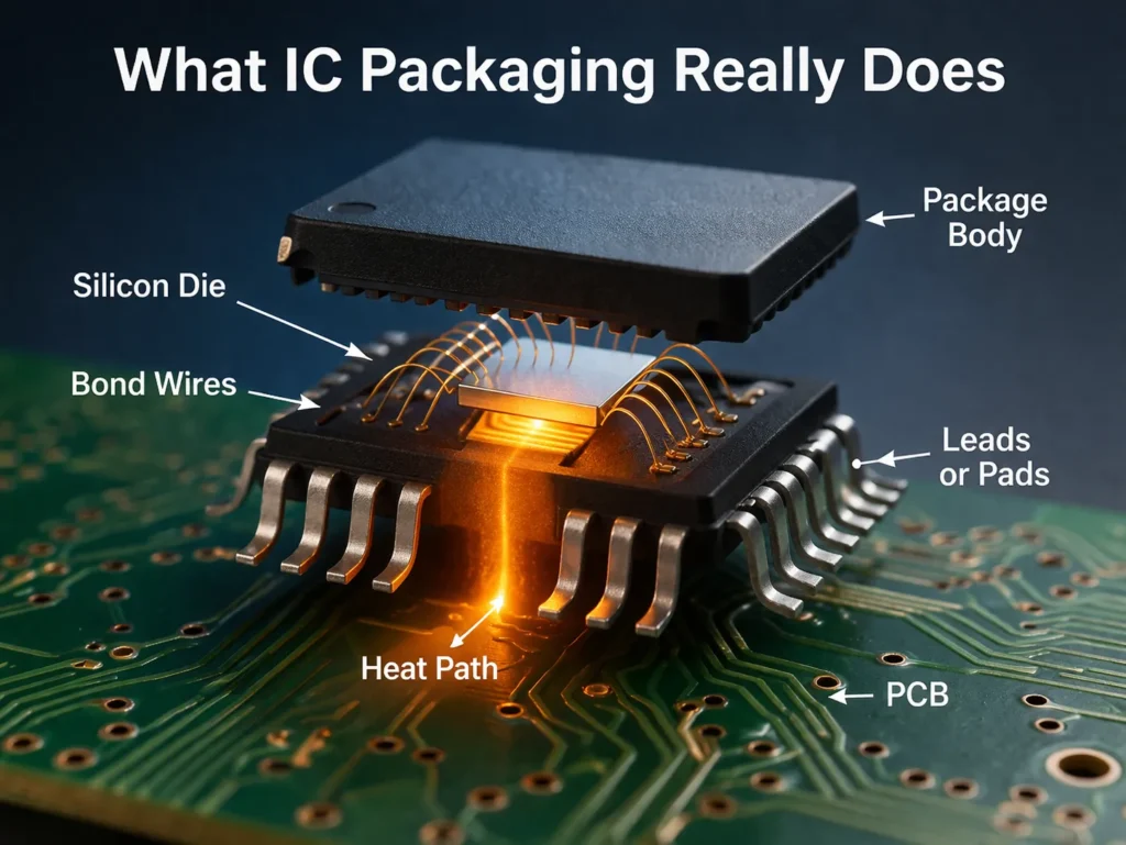
What IC Packaging Really Does
IC packaging is not just a protective enclosure. It gives the chip the physical and electrical interface it needs to work in a product. Your original version already framed this well around connectivity, protection, thermal dissipation, and manufacturability. In practice, an IC package determines four critical things:

Electrical Connectivity
The package connects the silicon die to external pins, leads, or pads. Package geometry affects parasitic inductance and capacitance, which directly matters for high-speed, analog, and RF behavior.
Mechanical Protection
The package protects the die from moisture, contamination, vibration, ESD, and mechanical stress.
Thermal Dissipation
The package provides the heat path from die to PCB and air. In many regulators and drivers, thermal performance can limit usable current more than the silicon itself.
Manufacturability
The package affects placement, soldering, inspection, rework, PCB routing, and assembly yield.
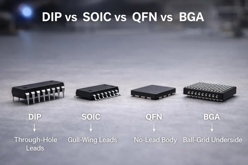
DIP vs SOIC vs QFN vs BGA: Which Package Should You Choose?
Many readers do not start by asking “what does packaging do?” They start with a comparison question. This quick matrix gives a faster answer than a thermal table alone.
| Package | Mounting Method | Hand Solderability | Thermal Performance | High-Speed Performance | Inspection Difficulty | Cost | Best Use Case |
|---|---|---|---|---|---|---|---|
| DIP | Through-hole | Excellent | Poor | Poor | Easy | Low to medium | Prototyping, education, legacy systems |
| SOIC | Surface mount | Good | Moderate | Moderate | Easy | Low | General-purpose analog and digital ICs |
| TSSOP | Surface mount | Fair | Moderate | Good | Easy to moderate | Low | Compact MCU, audio, interface, and controller designs |
| QFN | Surface mount, no-lead | Fair to difficult | Excellent | Excellent | Moderate to hard | Medium | PMICs, RF, motor drivers, compact high-performance boards |
| BGA | Surface mount, ball array | Poor | Excellent | Excellent | Hard | High | Processors, FPGAs, DDR, high pin count systems |
| WLCSP | Surface mount, wafer-level | Poor | Good | Excellent | Hard | Medium to high | Mobile, wearables, ultra-compact designs |
DIP is easiest for hand soldering. SOIC is the most forgiving general SMT choice. QFN is often the best balance for modern compact and thermally demanding designs. BGA is the right choice when pin count and high-speed performance matter most. WLCSP is for products where every millimeter counts.

Common IC Package Types
DIP (Dual In-Line Package)
Through-hole, mechanically robust, large inductance
DIP was once the dominant IC form factor and is still useful in prototyping, education, repair, and some legacy industrial systems. Your original article already notes that DIP is easy to solder and mechanically robust, but large and poor for high-speed work.
Best for: prototyping, breadboards, teaching, repair-friendly designs.
Main trade-off: large footprint and poor electrical parasitics compared with modern SMT packages.
SOIC (Small Outline Integrated Circuit)
Standard SMT package for low- to mid-pin-count ICs
SOIC remains one of the most practical all-purpose package types. It offers easier inspection and assembly than no-lead packages, and it still works well for many analog, digital, and mixed-signal devices. Your original article positions SOIC as low cost, easy to route, and widely manufacturable, which is exactly why it is still so common.
Best for: general-purpose ICs, analog devices, logic, EEPROMs, and designs that still need practical hand inspection.
TSSOP / SSOP
Compact, fine-pitch SMT with lower profile than SOIC
TSSOP and SSOP are useful when SOIC is too large but a more aggressive package like QFN is unnecessary. They reduce size and parasitics while staying easier to inspect than bottom-terminated packages. Your original version already covered their smaller pitch and their fit for MCUs, codecs, PMIC controllers, and interface ICs.
Best for: compact but still practical SMT assemblies.
QFN (Quad Flat No-Lead)
Low-parasitic, thermally efficient, modern standard for power and RF
QFN is one of the most important modern package families for PMICs, RF chips, microcontrollers, converters, and motor drivers. The exposed thermal pad and short signal path make it especially attractive where heat and parasitics matter. Your original article correctly highlights QFN’s thermal and electrical advantages, as well as the challenge of soldering the bottom pad well.
Best for: power ICs, RF, compact high-performance analog or mixed-signal boards.
BGA (Ball Grid Array)
High-speed, high-density package for processors, FPGAs, and memory
BGA is usually the right answer when the design needs very high I/O density and strong signal integrity for fast buses like DDR, PCIe, SerDes, or high-end SoCs. Your original article already positions BGA well for processors, FPGAs, DDR memory, and wireless SoCs, with the key downside being inspection and rework difficulty.
Best for: high pin count, high-speed digital systems.
WLCSP (Wafer-Level Chip Scale Package)
Smallest possible package for very space-constrained products
WLCSP minimizes footprint and parasitics, making it attractive for smartphones, wearables, and ultra-compact modules. But it is mechanically delicate and more demanding in assembly and reliability engineering. Your original article already flags PCB flex sensitivity and underfill requirements, which are important real-world caveats.
Best for: mobile electronics, wearables, tiny RF or PMIC subsystems.
Common Package Naming Conventions: SOIC, TSSOP, QFN, LQFP, BGA, WLCSP
One weakness in many package guides is that they cover only a few families. To better match how engineers search, this page should also mention several common naming conventions beyond the original core set. Your original article already covers the main six families, so this section broadens the search surface without replacing the main structure.
QFP / LQFP
Quad Flat Package families use gull-wing leads on all four sides. LQFP is a low-profile version. They are common for MCUs and controllers with moderate to high pin counts.
DFN
Dual Flat No-Lead packages are similar to QFN but with pads on two sides instead of four. Common in compact analog, PMIC, and sensor devices.
SOT-23 / SOT-23-5
Very small leaded packages commonly used for regulators, comparators, op-amps, and small-signal analog functions.
TO-220 / TO-252 / TO-263
Power-oriented packages designed for thermal dissipation and current handling. Often used for regulators, MOSFET drivers, and power semiconductors.
BGA Variants
FBGA, uBGA, and other variants are optimized for memory, compact digital packages, and high-density systems.
Chip-Scale Variants
WLCSP and related chip-scale packages are used when minimizing size and parasitics is the top priority.
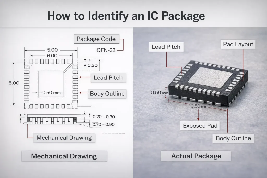
How to Identify an IC Package from the Datasheet
This is one of the most valuable additions for search intent, because many users are trying to identify a package rather than just learn definitions. Your original article explains what each package does, but it does not yet explicitly teach how to recognize them.

1) Look for the Package Outline Drawing
Most datasheets include a mechanical drawing near the end. This usually shows body dimensions, lead pitch, pad layout, overall footprint, and a package code.
2) Check the Package Code or Ordering Suffix
Manufacturers often encode the package in the part number suffix. The same IC may be offered in SOIC, TSSOP, QFN, or BGA versions under slightly different ordering codes.
3) Count Pins and Look at Lead Style
- DIP: two long through-hole rows
- SOIC/TSSOP: visible gull-wing leads on two sides
- QFP/LQFP: gull-wing leads on four sides
- QFN/DFN: no protruding leads, pads under the body edge
- BGA: solder balls under the package
- WLCSP: tiny bump array, almost die-sized
4) Compare the Product Photo to Known Package Shapes
If you only have a supplier image or product photo, the easiest clues are package body shape, visible leads, pad arrangement, and pin count distribution.
5) Check the Recommended Land Pattern
The PCB footprint recommendation often makes package identification much easier. A visible exposed pad usually points to QFN or DFN. Four-sided leads usually indicate QFP. A ball array indicates BGA.
If you are unsure whether a package is QFN or DFN, check how many sides have pads. If you are unsure whether it is SOIC or TSSOP, check the pitch and body width. If you are unsure whether it is QFP or BGA, look for visible leads versus hidden solder balls.
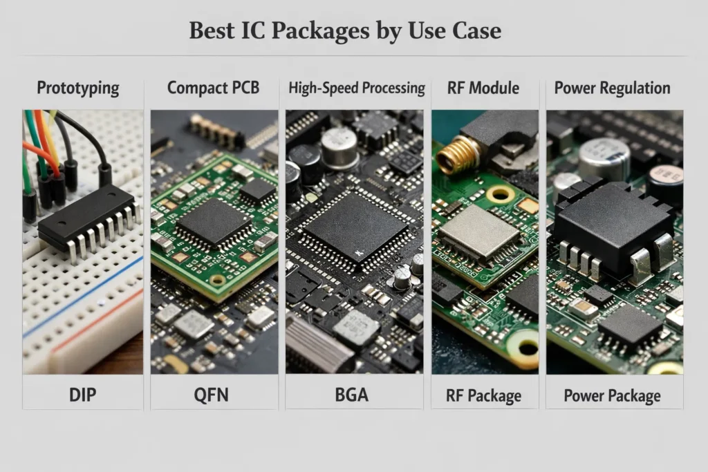
Best IC Packages for Prototyping, Mass Production, and High-Speed Design
| Use Case | Best Package Choices | Why |
|---|---|---|
| Prototyping and education | DIP, SOIC | Easy to solder, inspect, and rework |
| Low-cost mass production | SOIC, TSSOP | Good manufacturability and broad assembler support |
| Compact consumer electronics | QFN, DFN, WLCSP | Small footprint and good electrical behavior |
| Power regulation and thermal load | QFN, TO-220, TO-263, BGA | Better thermal path and current handling |
| High-speed digital systems | BGA, QFN | Lower parasitics and stronger signal integrity |
| RF and wireless design | QFN, WLCSP, DFN | Low inductance and compact signal path |

Thermal Performance of IC Packages
Thermal behavior is one of the most important package-selection variables. Your original article already includes a useful thermal comparison table built around θJA and θJC, which is exactly the right engineering foundation.
| Package | θJA (Typical) | θJC (Typical) | Thermal Notes |
|---|---|---|---|
| DIP | 80–120°C/W | 20–40°C/W | Weak thermal path, not ideal for thermally stressed ICs |
| SOIC | 60–100°C/W | 15–30°C/W | PCB copper improves performance |
| TSSOP | 50–90°C/W | 12–25°C/W | Compact but not a true thermal package |
| QFN | 25–50°C/W | 1–5°C/W | Exposed pad gives strong thermal transfer |
| BGA | 20–40°C/W | 1–3°C/W | Strong heat spreading through ball grid and PCB |
| WLCSP | 40–70°C/W | 2–5°C/W | Short path, but total performance depends on board and die size |
Electrical Parasitics and Signal Integrity
Your original article already explains that lead length, pad size, internal bond approach, and overall geometry affect package parasitics. That matters because package parasitics influence:
- Overshoot and ringing
- Bandwidth and rise time
- Noise pickup and EMI behavior
- RF matching performance
- ADC, DAC, and clock signal integrity
As a rule, DIP and other long-lead packages are the weakest for high-speed work, while QFN, BGA, and WLCSP are much better choices when parasitics must be minimized.
Manufacturing and Reliability Considerations
Your original version already covers MSL, reflow profiles, solder-joint reliability, and mitigation strategies like underfill and symmetric copper distribution. Those topics are important because package selection is never only about electrical specs.
MSL Risk
DIP and SOIC are usually easier to manage. QFN may need tighter handling control. BGA and WLCSP often require the most disciplined moisture handling.
Inspection
Leaded packages are easier to inspect visually. Bottom-terminated and ball-array packages often require X-ray or more advanced QA methods.
Rework
SOIC and TSSOP are far easier to rework than BGA or WLCSP. QFN sits in the middle but still demands care.
Mechanical Reliability
BGA and WLCSP are more sensitive to drop shock, flex, and thermal cycling, which is why underfill and layout symmetry matter.
How to Select the Right IC Package
Your original article already groups package choice by electrical requirements, thermal load, mechanical environment, manufacturing capability, and cost, which is exactly the right framework. Here is the simplified decision version:
- Choose DIP when easy prototyping and hand soldering matter most.
- Choose SOIC or TSSOP when you need practical SMT assembly and reasonable cost.
- Choose QFN or DFN when compact size, thermal performance, and signal integrity matter.
- Choose BGA when pin count and high-speed digital performance dominate the design.
- Choose WLCSP only when size is critical and the manufacturing process can support it.
- Choose TO-style packages for discrete-like power handling and thermal dissipation needs.
Related Reading on MOZ Electronics
FAQ: IC Package Types
What is an IC package?
An IC package is the physical enclosure and connection structure around a semiconductor die. It determines how the chip mounts, cools, connects electrically, and survives assembly and field use.
What is a SOIC package?
SOIC stands for Small Outline Integrated Circuit. It is a common surface-mount package with gull-wing leads on two sides, widely used for analog, logic, and mixed-signal ICs.
What is a QFN package?
QFN stands for Quad Flat No-Lead. It is a compact package with pads around the underside edge and usually an exposed thermal pad, making it strong for compact, thermal, and RF-sensitive designs.
DIP vs SOIC: which is easier to solder?
DIP is easier for hand soldering and breadboard use. SOIC is still manageable, but it is meant for surface-mount assembly rather than through-hole prototyping.
BGA vs QFN: which is better?
BGA is better when you need very high pin count and strong high-speed performance. QFN is better when you need a compact, lower-parasitic, thermally efficient package without the complexity of a ball-grid array.
Which IC package is easiest to solder?
DIP is the easiest, followed by SOIC. TSSOP is still manageable with care. QFN, BGA, and WLCSP are progressively more difficult and usually require stronger process control.
Conclusion
IC package selection is not just a mechanical afterthought. It shapes thermal performance, parasitic behavior, solderability, inspection flow, rework difficulty, and long-term reliability. The strongest package choice depends on what the design actually needs: easy prototyping, low-cost production, compact size, high-speed signaling, RF performance, or heat dissipation.
As a package-focused hub page, this article should answer both engineering and search-intent questions: what the package is, how to compare the major families, how to identify a package in a datasheet, and how to choose the right one for a real design.


