When designing high-precision measurement or control systems, digital-to-analog conversion (DAC) is often the final step in transforming digital data into meaningful analog signals. For FPGA-based designs, pairing your FPGA with a reliable, low-noise, 16-bit DAC such as the Analog Devices AD5541 ensures stable, accurate analog outputs that can be used in test equipment, automation, medical devices, and laboratory instruments.
This guide provides a complete overview of AD5541 FPGA integration, including wiring, SPI communication setup, calibration techniques, PCB layout best practices, and long-term maintenance tips. Whether you are an engineer working on sensor calibration, signal synthesis, or control systems, this tutorial will help you achieve the most from your AD5541 + FPGA setup.
AD5541 FPGA Basics
The AD5541 is a single-channel, 16-bit DAC with an unbuffered voltage output. It is widely used because of its precision, fast settling time, and compatibility with standard serial communication protocols.
Key Features of AD5541
| Specification | Details |
|---|---|
| Resolution | 16-bit |
| Architecture | R-2R ladder |
| Output Type | Unbuffered voltage output |
| Supply Voltage | 2.7 V – 5.5 V |
| Settling Time | 1 µs |
| INL/DNL | ±0.5 LSB |
| Noise Density | 11.8 nV/√Hz |
| Power Consumption | 0.625 mW at 5 V, 0.375 mW at 3 V |
| Interface | 3-wire SPI/QSPI/Microwire/DSP compatible |
| Package | 8-SOIC |
The DAC is monotonic over the entire temperature range (−40°C to +85°C), ensuring predictable and accurate behavior in industrial and scientific environments.
Tip: The AD5541 is optimized for unipolar outputs (0 V to VREF). If you need bipolar operation (±VREF), the AD5542 is a better option.
Wiring AD5541 to FPGA
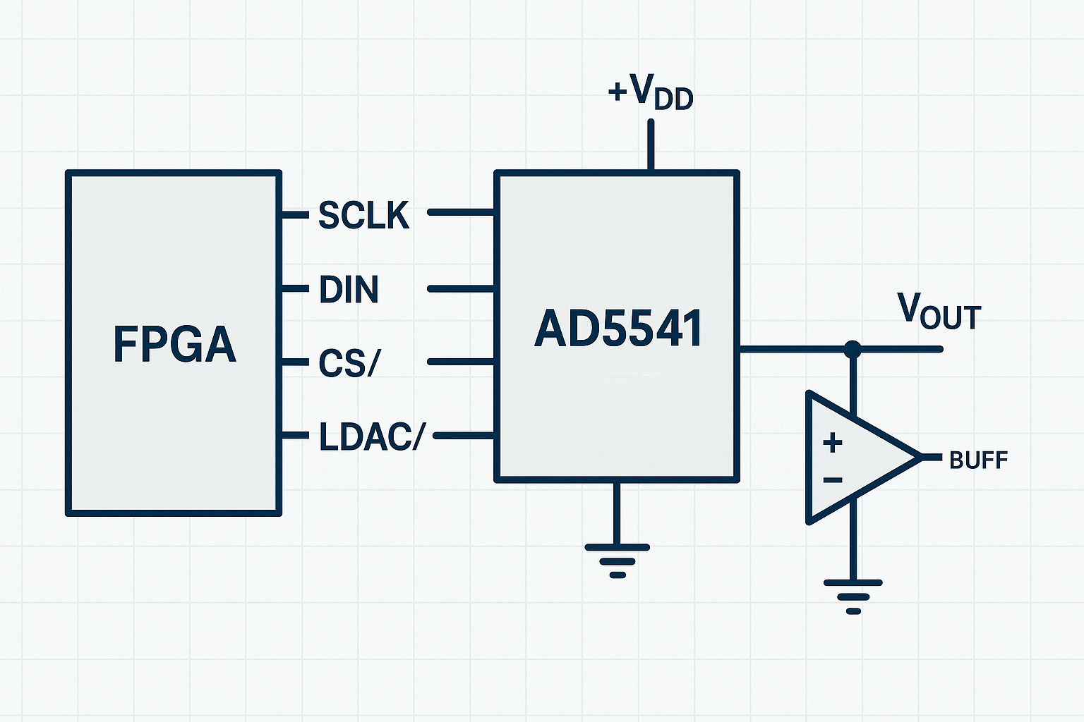
Integrating the AD5541 with an FPGA requires careful wiring to maintain signal integrity. The SPI interface simplifies connectivity, using just a few lines.
Pin Mapping

| FPGA Signal | AD5541 Pin | Description |
|---|---|---|
| SCLK | Serial Clock | Provides the timing clock |
| DIN | Data Input | Serial input, MSB first |
| ~CS | Chip Select | Enables DAC input when low |
| ~LDAC | Load DAC | Updates DAC output when low |
| VDD | Power | 2.7–5.5 V supply |
| GND | Ground | Must be tied to FPGA ground |
Power and Ground
- Use a stable supply voltage within 2.7 V–5.5 V.
- Place 0.1 µF and 10 µF decoupling capacitors close to VDD.
- Tie FPGA and DAC grounds together for correct logic level reference.
- Keep analog and digital grounds carefully managed to reduce noise.
SPI Communication Setup
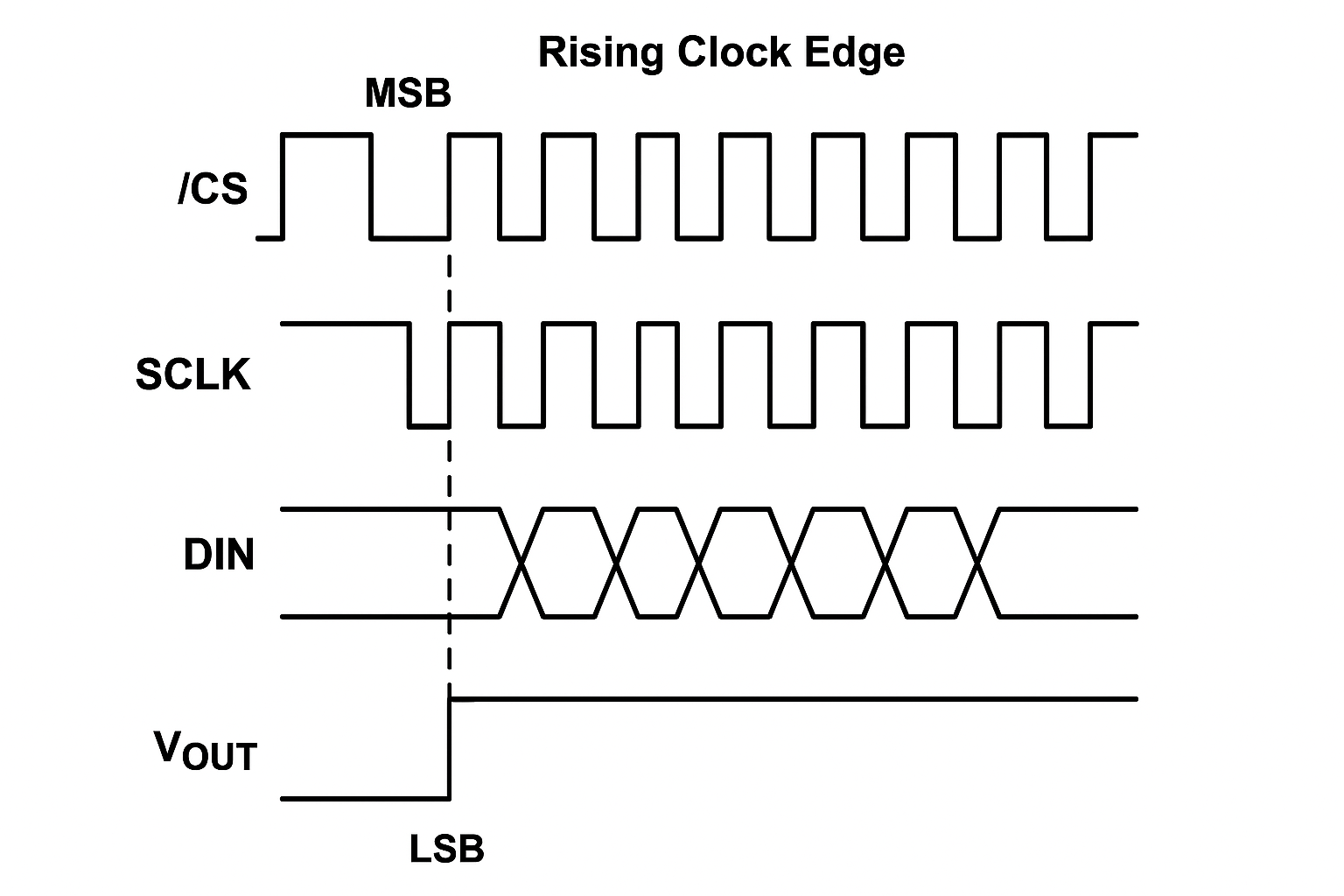
The AD5541 uses a simple 3-wire SPI protocol.

SPI Mode
- Mode 0 (CPOL = 0, CPHA = 0)
- Data is sampled on the rising edge of SCLK.
- CS must remain low during the full 16-bit transfer.
Timing Diagram Essentials
- Pull CS low.
- Send 16-bit word (MSB first) on DIN.
- Data is latched on each rising edge of SCLK.
- Bring CS high after transfer to update register.
- LDAC low → output updates immediately.
Example FPGA Code
Verilog Example: SPI Controller for AD5541
module ad5541_spi(
    input wire clk,          // System clock
    input wire reset,        // Reset
    input wire [15:0] data,  // 16-bit input data
    input wire start,        // Start transfer
    output reg sclk,         // SPI clock
    output reg din,          // Data out
    output reg cs,           // Chip select
    output reg busy          // Busy flag
);

reg [4:0] bit_cnt;
reg [15:0] data_buf;

always @(posedge clk or posedge reset) begin
    if (reset) begin
        cs <= 1'b1;
        sclk <= 1'b0;
        din <= 1'b0;
        busy <= 1'b0;
        bit_cnt <= 0;
        data_buf <= 0;
    end else begin
        if (start && !busy) begin
            cs <= 1'b0;
            busy <= 1'b1;
            bit_cnt <= 16;
            data_buf <= data;
        end else if (busy) begin
            sclk <= ~sclk;
            if (sclk == 1'b0) begin
                din <= data_buf[15];
                data_buf <= {data_buf[14:0], 1'b0};
                bit_cnt <= bit_cnt - 1;
            end else if (bit_cnt == 0) begin
                cs <= 1'b1;
                busy <= 1'b0;
                sclk <= 1'b0;
            end
        end
    end
end
endmodule
This module ensures proper SPI timing, handling chip select, data shifting, and clock toggling.
Calibration and Testing
Calibration Steps
- Send known 16-bit values from FPGA.
- Measure DAC output with oscilloscope or multimeter.
- Compare measured values with theoretical
Vout = (Code / 65536) * VREF. - Adjust FPGA scaling factors if necessary.
- Repeat across full DAC range.
| Step | Action |
|---|---|
| 1 | Send digital code |
| 2 | Measure analog output |
| 3 | Compare expected vs actual |
| 4 | Adjust FPGA scaling/offset |
| 5 | Repeat for multiple points |
Testing Tools
- Oscilloscope → check analog output shape and noise.
- Logic analyzer → validate SPI timing.
- Protocol analyzers → debug miscommunication.
PCB Layout and Noise Reduction
For high-precision systems, PCB design is as important as HDL code.
Layout Tips
- Place AD5541 close to FPGA.
- Keep SPI traces short and direct.
- Separate analog and digital ground planes.
- Use solid ground plane underneath DAC.
- Avoid sharp 90° trace bends.
Noise Reduction Strategies
| Technique | Benefit |
|---|---|
| Decoupling capacitors (0.1 µF + 10 µF) | Block supply noise |
| Shielded analog traces | Reduce EMI |
| Twisted pair wires | Cancel noise coupling |
| Buffer op-amp (≥1 MHz bandwidth) | Ensure stable output drive |
| Oversampling & filtering | Lower jitter and quantization noise |
AD5541 FPGA Application Scenarios
The AD5541 FPGA combination is widely used in:
- Sensor Calibration – convert FPGA-processed signals into precise voltages for sensor tuning.
- Test Equipment – generate reference waveforms for measurement systems.
- Industrial Automation – control actuators, motors, and analog control loops.
- Medical Devices – produce stable analog voltages for signal conditioning.
- Lab Instruments – precise waveform synthesis and lock-in detection.
Best Practices for Long-Term Accuracy
Reliability Guidelines
- Use precision voltage reference (low drift).
- Employ low-noise LDO regulators.
- Regularly recalibrate system.
- Monitor temperature effects on DAC.
- Maintain clean PCB (dust, oxidation reduce reliability).
Common Error Sources
| Error Type | Description | Mitigation |
|---|---|---|
| Saturation | Output limited near supply rails | Use op-amps with higher headroom |
| Timing Errors | SPI misalignment | Check timing with analyzer |
| Resistance Drift | Causes nonlinearity | Use stable resistors and recalibration |
| Rds-on Variations | Output driver mismatch | Apply filters and higher supply margin |
FAQ About AD5541 FPGA
Q1: How do I connect AD5541 to an FPGA?
To connect the AD5541 DAC to an FPGA, link the four main SPI lines: SCLK for the clock, DIN for data, CS as the chip select, and LDAC to update the output. Power the DAC with a stable 2.7–5.5 V supply and tie the grounds of both devices together for consistent logic levels. Keep all wires as short as possible to reduce noise and signal delay. If needed, place a buffer op-amp on the output to handle heavier loads. A clean, simple wiring layout ensures accurate and stable analog performance.
Q2: What SPI mode does AD5541 use?
The AD5541 communicates using SPI mode 0, meaning the clock idles low and the DAC samples data on the rising clock edge. Each transfer requires a 16-bit word, with the most significant bit sent first. The chip select line must remain low for the entire transfer, then go high to latch the data. Keeping LDAC low allows automatic updating after every frame, while pulsing it gives precise control over when the analog output changes. Following these timing rules ensures reliable digital-to-analog conversion.
Q3: Why do I need decoupling capacitors near the DAC?
Decoupling capacitors are essential because they stabilize the power supply and prevent unwanted noise from reaching the DAC. A small ceramic capacitor (0.1 µF) placed close to the DAC pin filters high-frequency noise, while a larger capacitor (4.7–10 µF) smooths low-frequency variations. Together, they ensure the voltage rail remains steady, even during sudden current changes. This keeps the analog output accurate, reduces ripple, and improves long-term stability. Without proper decoupling, the DAC output can drift or become noisy, especially in sensitive applications.
Q4: How can I test if my AD5541 FPGA setup is working?
Testing begins by sending known digital values from the FPGA and measuring the DAC’s analog output. For example, sending code 0x0000 should give 0 V, while 0x8000 should give roughly half of VREF, and 0xFFFF should approach the reference voltage. Compare measured voltages with the expected formula Vout=Code/65536×VREFVout = Code/65536 × VREFVout=Code/65536×VREF. If results differ, adjust scaling or wiring. Using an oscilloscope or logic analyzer helps confirm SPI timing. This step-by-step validation ensures both the digital communication and analog conversion are functioning properly.
Q5: What’s the difference between AD5541 and AD5542?
The AD5541 provides a unipolar output range from 0 to VREF, making it ideal for simple voltage generation. The AD5542, however, offers additional flexibility by supporting bipolar operation (±VREF) and including Kelvin sense pins for improved reference and ground accuracy. This means the AD5542 can deliver symmetrical positive and negative outputs, which is useful for test equipment and instrumentation. If your design only requires positive voltages, the AD5541 is sufficient; but if you need bipolar swing and tighter precision, the AD5542 is the better choice.
Q6: How do I reduce noise in my DAC output?
To minimize noise, start with a clean power supply and place decoupling capacitors close to the DAC. Keep SPI and analog traces short, and separate digital and analog paths on the PCB to avoid interference. A solid ground plane helps stabilize signals, while shielding sensitive lines further reduces noise pickup. For applications that demand very low noise, you can add a buffer amplifier and a simple RC low-pass filter at the output. These steps ensure smooth, stable analog signals suitable for precision measurement and control systems.
Conclusion
Integrating the AD5541 DAC with FPGA provides engineers with a robust solution for generating accurate, stable analog signals. With correct wiring, proper SPI configuration, systematic calibration, and good PCB layout practices, you can achieve 16-bit precision with minimal noise and drift.
For more resources, refer to:
By following this guide, your AD5541 FPGA system will deliver reliable performance in sensor calibration, automation, test instruments, and medical electronics.


