If you’ve ever built a breadboard project, debugged a small amplifier, or switched a relay from a microcontroller, chances are you’ve used (or could have used) the 2N3904. This humble, inexpensive NPN bipolar junction transistor (BJT) has been a go-to choice for decades because it’s easy to drive, tolerant of hobbyist abuse, and available from practically every supplier in TO-92 through-hole and SMD variants.
This guide gives you everything you need to use the 2N3904 confidently: pinout, key specs from the datasheet, design equations, worked examples (LED driver, logic-level switch, common-emitter amplifier), layout and thermal tips, and quick comparisons to close cousins like the 2N2222 and MMBT3904.
What the 2N3904 is (and isn’t)
The 2N3904 is a general-purpose, small-signal NPN BJT designed for low-power amplification and switching. It’s the complement to the PNP 2N3906; together they cover many push-pull and general analog tasks. Historically registered by Motorola in the 1960s, it helped popularize plastic TO-92 encapsulation for cost and performance reasons. Today, it’s still widely produced by multiple manufacturers. (Wikipedia)
Where it shines
- Logic-level low-side switching up to a couple hundred milliamps
- Simple audio/sensor preamps and signal buffering up to RF-adjacent frequencies
- Level shifting, small relay/solenoid drivers (with proper protection), LED driving
Where not to use it
- High-power loads (look at power BJTs or MOSFETs)
- High-voltage beyond tens of volts (use dedicated high-voltage parts)
- Precision low-noise instrumentation front-ends that specify ultra-low flicker noise
2N3904 Pinout (TO-92)
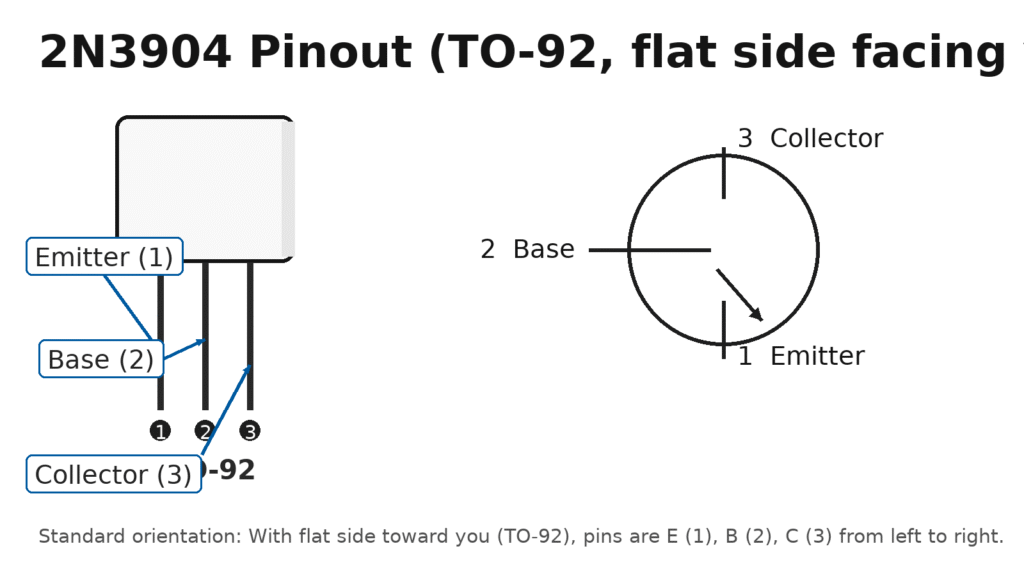
Face the flat side of the TO-92 package with leads downward. From left to right the pins are: Emitter (E), Base (B), Collector (C). This E-B-C ordering is standardized for genuine 2N3904 parts. Some manufacturers even mark “EBC” on the molding.

SMD equivalents:
- MMBT3904 in SOT-23
- PZT3904 in SOT-223 (higher thermal dissipation)
Package-dependent power ratings vary (≈0.625 W for TO-92, up to ~1 W for larger SMD packages with heatsinking).
Key Electrical Specifications (from the ON Semiconductor 2N3904 datasheet)
A few headline numbers you’ll reach for often:
- VCEO (Collector-Emitter voltage): 40 V
- VCBO: 60 V; VEBO: 6 V
- IC (continuous collector current): 200 mA
- Power dissipation (TO-92): 625 mW @ 25 °C, derate 5 mW/°C
- hFE (DC gain): typ. 100–300 @ IC=10 mA
- fT (gain-bandwidth): ~300 MHz at IC=10 mA, VCE=20 V, f=100 MHz
- Switching: ~35 ns rise and delay, ~50 ns fall, ~200 ns storage (typical test conditions)
- Junction temperature range: –55 to +150 °C
All of the above are taken directly from ON Semiconductor (onsemi)’s current datasheet revision (Oct 2024) and its Electrical Characteristics table/graphs.
Note: Older or third-party PDFs sometimes quote fT=250–270 MHz at similar conditions—differences reflect process and measurement conditions. The latest onsemi sheet lists 300 MHz at the specified test point.
2N3904 vs 2N2222
Both are ubiquitous NPNs. The 2N2222 (and PN2222A) tends to have stronger current capability and lower VCE(sat) at higher currents; the 2N3904 is great at small-signal tasks and is widely available, often with higher fT/low capacitances suited to RF/IF or high-speed switching in the low-current regime. If you’re switching a relay coil or need margin at > 150 mA, the 2N2222 is often a safer bet; for general analog and logic interfacing, the 2N3904 is excellent.
SMD naming: MMBT3904 (SOT-23) and PZT3904 (SOT-223) are the 2N3904 in surface-mount clothing; dissipation differs by package and PCB copper.
2N3904 Datasheet Highlights You Should Know
Here are the most useful table entries and why they matter (from the onsemi Oct-2024 datasheet):
- VCEO=40 V, VCBO=60 V, VEBO=6 V — absolute voltage limits for safe operation.
- IC=200 mA (continuous) — practical upper bound for load current.
- hFE: 100–300 @ 10 mA — gives you a feel for biasing targets in analog designs; don’t use this for switching margins.
- VCE(sat): 0.3 V typ @ IC=50 mA, IB=5 mA — check drop and dissipation in saturation.
- fT =300 MHz @ 10 mA, 20 V — useful for estimating small-signal bandwidth potential.
- td, tr, ts, tf in tens to hundreds of ns — a quick read on switching speed class.
- PD=625 mW, RθJA≈200 °C/W — sanity checks for thermal calculations.
If you purchase non-onsemi variants, expect similar limits but always re-check the actual vendor’s datasheet for pinout drawings, binning, and thermal data (e.g., ST’s sheet shows fT=250–270 MHz at the same test point).
Conclusion
The 2N3904 endures because it hits the sweet spot: easy to bias, fast enough for a huge range of small-signal jobs, cheap, and in every toolbox. If your project needs a general-purpose NPN under 200 mA and 40 V, start with the 2N3904. For heavier loads, step up to 2N2222 or a small MOSFET; for SMD, use MMBT3904. And whenever you’re unsure, open the latest manufacturer datasheet—that one page of numbers will save you hours later.
FAQ About 2N3904 + its Complement 2N3906
Q: What’s the absolute max current I can switch with a 2N3904, and what about the 2N3906?
A: For the 2N3904 (NPN), the datasheet continuous collector current is typically 200 mA. Design with margin—≤150 mA is a good comfort zone—and check heating using P ≈ VCE(sat) · IC. The 2N3906 (PNP) has a similar ballpark current rating for small-signal jobs, but remember it’s used as a high-side device in many cases; ensure you respect VEBO, VCEO and dissipation just as you would with the 2N3904.
Q: Can I drive a 2N3904 from a 3.3 V GPIO? Can I do the same with a 2N3906?
A: Yes. For a 2N3904 low-side switch, size the base resistor with a forced β (e.g., 10):
- Example: want IC=50 mA, βforced=10 → IB=5 mA.
- With VCTRL=3.3 V and VBE(sat)≈0.85–0.95 V, RB≈(3.3−0.9)/0.005≈480 Ω → use 470 Ω (if your MCU can source 5 mA). If not, either reduce IC, increase RB, or buffer the pin.
For a 2N3906 high-side switch from a 3.3 V GPIO, the base drive polarity inverts: you pull the base low (below the emitter) to turn it on. Compute RB the same way, but be sure your logic can pull the base sufficiently below VE (and mind any level-shifting needed if the emitter sits at 5 V while the MCU is 3.3 V).
Q: Does the pinout ever change for 2N3904/2N3906?
A: In TO-92, genuine parts are almost always E–B–C left-to-right with the flat face toward you for both 2N3904 and 2N3906. Still, check the specific vendor drawing—counterfeits and other transistor families can swap C and E. For SOT-23 (MMBT3904/MMBT3906), verify the pin mapping in the SMD datasheet before laying out your board.
Q: What are the common SMD versions of 2N3904 and 2N3906?
A:
- 2N3904 → MMBT3904 (SOT-23); higher-dissipation variant PZT3904 (SOT-223) exists.
- 2N3906 → MMBT3906 (SOT-23); similarly, PZT-style packages exist from some vendors.
Remember that package greatly affects power dissipation (and RθJA). A PZT device on a copper pour can handle far more heat than a TO-92 dangling in air.
Q: Which PNP part complements the 2N3904, and how do I use the pair together?
A: The complementary PNP is 2N3906. Together they form push-pull stages (e.g., emitter followers for buffering) or class-AB small-signal outputs. In a basic complementary emitter follower:
- 2N3904 sources current to ground (sinks load current).
- 2N3906 sources current from V+.
- Add biasing (two diodes or a VBE-multiplier) to reduce crossover distortion, and include emitter resistors (10–100 Ω) for thermal sharing and stability.
Q: For LED driving, should I pick 2N3904 or 2N3906?
A: For a low-side LED switch, choose 2N3904: LED anode to +V through a series resistor, LED cathode to the 2N3904 collector, emitter to ground. The 2N3906 is the mirror image for high-side LED switching: emitter to +V, collector to LED anode, LED cathode to resistor then ground—mind that the base drive must pull lower than the emitter to turn it on.
Q: What about voltage limits for 2N3904 vs. 2N3906?
A: Typical limits are similar: VCEO ≈ 40 V, VCBO ≈ 60 V, VEBO ≈ 6 V for both 2N3904 and 2N3906 families (check your specific datasheet). Never exceed VEBO; add a base-emitter clamp (small signal diode) if transients might push the junction into reverse breakdown.
Q: How do saturation and hFE compare between 2N3904 and 2N3906?
A: Both are general-purpose devices with mid-range hFE (≈100–300 around 1–10 mA). In switching, always use forced β (10–20) for either device to guarantee saturation across temperature and part-to-part spread. Expect VCE(sat) in the 0.1–0.3 V range at tens of mA when driven hard; the exact number depends on current and base overdrive.
Q: Can I replace a 2N3904 with a 2N3906 (or vice versa) if I flip the supply?
A: Not drop-in. They are complements, not substitutes. A 2N3904 is NPN (current flows collector → emitter with the base forward-biased), while 2N3906 is PNP (current flows emitter → collector). Swapping one for the other usually requires changing polarities, bias voltages, and possibly signal inversion. In many designs you’d use both to get symmetric push-pull behavior.
Q: What are good starting bias currents for small-signal amplification with 2N3904/2N3906?
A: For wide small-signal bandwidth and decent noise, bias around 1–5 mA. The 2N3904 often shows fT ~ 250–300 MHz near ~10 mA; the 2N3906 is similar in class but typically a bit lower in RF performance—still perfectly fine for audio and many IF tasks. Always verify your specific vendor curves.
Q: Any special protection needed when using 2N3904 or 2N3906 on inductive loads (relays, motors)?
A: Yes. With 2N3904 as a low-side driver, put a flyback diode across the coil (cathode to +V, anode to the transistor collector). With 2N3906 as a high-side driver, place the diode appropriately (cathode to the transistor emitter/+V, anode to the load side). This protects both devices from voltage spikes that can exceed VCEO.
Q: How do I pick base resistors for a push-pull buffer using 2N3904 + 2N3906?
A: Treat each transistor separately: decide the peak load current you expect each half to handle, apply βforced (e.g., 10–20), then compute RB from the drive voltage to get that base current at the extremes of the waveform. Add small emitter resistors (10–100 Ω) to linearize and prevent thermal runaway; consider diode biasing between bases to reduce crossover.
Q: Are there SMD drop-ins for both 2N3904 and 2N3906 that keep the “complement” relationship?
A: Yes—MMBT3904 (NPN) pairs with MMBT3906 (PNP) in SOT-23. They’re widely available, inexpensive, and retain the complementary behavior of the through-hole pair. Check your PCB library symbols and pin mapping before fabrication.
Q: Any ESD or base-emitter reverse-bias gotchas specific to 2N3904/2N3906?
A: Both parts have VEBO ≈ 6 V max and can be damaged by reverse base-emitter stress. If the base node might see negative or over-voltage transients (relative to the emitter), add a clamp diode (e.g., 1N4148) across B–E in the blocking direction, and include series resistance from the driving source.
Sources and Datasheets
- ON Semiconductor (onsemi) 2N3904 datasheet, Rev. 3 (Oct 2024): ratings, characteristics, pin labeling and package details. Mouser Electronics
- Wikipedia: history, complementary part (2N3906), standardized E-B-C pin order and package notes, package variants (MMBT/PZT).
- STMicroelectronics 2N3904 PDF (SparkFun mirror): corroborating max ratings and typical fT =250–270 MHz figures. cdn.sparkfun.com
- Retailer summary/spec snapshots for context (part naming and availability): SparkFun product page. sparkfun.com


