


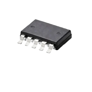
SN74HC595ADBR TI SN74HC595ADBR – High-Reliability 8-Bit Shift Register with Tri-State Output Buffers
- Industrial Temperature Range (-40°C to +85°C) for harsh environment operation
- Higher Output Drive Capacity (±6mA at 5V) vs basic 74HC logic family
- Robust ESD Protection (2000V HBM) for improved field reliability
SN74HC595ADBR Shift Register – Enhanced Version of Classic 74HC595 Optimized for Industrial & Harsh Environments
The SN74HC595ADBR IC from Texas Instruments represents the premium industrial-grade variant of the ubiquitous 74HC595 shift register. Designed for mission-critical applications where reliability is paramount, this enhanced version features:
- TI’s proprietary HC process technology optimized for noise immunity
- Wider operating voltage range (2V to 6V) compatible with 3.3V/5V systems
- 3-state output buffers with bus hold circuitry to prevent floating inputs
As part of TI’s extended reliability portfolio, the “A” suffix denotes strict manufacturing controls exceeding standard commercial-grade specifications – ideal for industrial automation, automotive, and medical equipment applications.
Technical Specifications
| Parameter | Specification |
|---|---|
| Base Product Number | 74HC595 |
| Supply Voltage Range | 2.0–6.0V |
| Max Clock Frequency (@5V) | 25MHz (SN74HC595ADBR) vs. 20MHz (Standard) |
| Output Drive Current | ±6mA (ADBR) vs. ±4mA |
| Propagation Delay | 13ns (ADBR) vs. 18ns |
| ESD Protection (HBM) | 2000V (ADBR) vs. 1000V |
| Operating Temp. Range | -40°C to +85°C (ADBR) vs. 0°C to +70°C |
Key Performance Advantages:
- Performance Boost:
- The SN74HC595ADBR offers 25% faster clock speed (25MHz vs. 20MHz) and 33% lower propagation delay (13ns vs. 18ns).
- Robustness:
- 2× better ESD protection (2000V vs. 1000V) and wider temperature range (-40°C to +85°C).
- Drive Strength:
- 50% higher output current (±6mA vs. ±4mA), enabling better load driving capability.
For designs requiring higher speed, ruggedness, or industrial environments, the SN74HC595ADBR is the superior choice.
Applications
1. Industrial Control Systems
- Motor control panels – Daisy-chain multiple units to drive dozens of relays/indicators
- PLC I/O expansion – Add digital outputs without microcontroller pin constraints
- HMI interfaces – Multiplex LEDs/keypads in hazardous locations
Example: In factory automation, 16x SN74HC595ADBR devices can control 128 safety interlock indicators via a single SPI bus, with the extended temp range ensuring operation near heat-generating equipment.
2. Automotive Electronics
- Cluster displays – Drive segment LCDs with minimal wiring
- Body control modules – Window/lock actuator control
- EV battery monitoring – Cell voltage indicator arrays
Implementation Note: The 2V low-voltage operation allows direct interface with 3.3V automotive microcontrollers without level shifters.
3. Medical Equipment
- Patient monitoring – Multiplex status LEDs on portable devices
- Diagnostic systems – Parallel data buffering for sensor arrays
- Therapy devices – Safe output isolation via tri-state control
Reliability Feature: Latch-up immunity exceeds 250mA per JESD78 Class II – critical for life-support equipment.
Functional Deep Dive
Enhanced Architecture
Compared to the standard SN74HC595:
- Reinforced Output Stage
- Dual-diode clamps on all outputs
- Current-limited drivers prevent damage during short circuits
- Improved Clock Tree
- Lower skew between SRCLK and RCLK paths
- Schmitt trigger inputs for noisy environments
- Manufacturing Enhancements
- 100% production testing at temperature extremes
- Burn-in sampling for high-reliability applications
Typical Performance Curves
(Reference datasheet 0900766b812cd41f.pdf, section 6.9)
- Propagation delay vs Vcc – Maintains <15ns across full voltage range
- ICC vs Temperature – Leakage current remains <100µA at 85°C
Comparison to Similar Devices
| Part Number | Temp Range | Max Freq | Drive | Key Differentiator |
|---|---|---|---|---|
| SN74HC595ADBR | -40°C+85°C | 25MHz | ±6mA | Industrial reliability |
| SN74HC595DBR | 0°C+70°C | 20MHz | ±4mA | Standard commercial |
| CD74HC595 | -55°C+125°C | 15MHz | ±4mA | Military qualified |
- For cost-sensitive designs → SN74HC595DBR
- Extreme environments → CD74HC595
- Optimal balance → SN74HC595ADBR
Key Variants Breakdown
| Variant | Package | Max Freq. (MHz) | Output Drive (mA) | ESD (V) | Temp. Range (°C) | Best For |
|---|---|---|---|---|---|---|
| SN74HC595N (Legacy DIP) | PDIP-16 | 20 @5V | ±4 | 1000 | 0 to +70 | Prototyping |
| SN74HC595D (Standard) | SOIC-16 | 20 @5V | ±4 | 1000 | 0 to +70 | Cost-sensitive PCBs |
| SN74HC595PW (Compact) | TSSOP-16 | 20 @5V | ±6 | 2000 | -40 to +85 | Dense PCB designs |
| SN74HC595ADBR (Enhanced) | SSOP-16 | 25 @5V | ±6 | 2000 | -40 to +85 | Industrial/high-speed apps |
| SN74HC595BQAR (Automotive) | QFN-16 | 29 @5V | ±6 | 2000 | -40 to +125 | Automotive/harsh env. |
Summary of Key Differences
- Speed:
- Standard variants (N/D/PW): 20MHz
- Enhanced (ADBR): 25MHz
- Automotive (BQAR): 29MHz (fastest)
- Drive Strength:
- Most variants: ±4mA (except ADBR/PW/BQAR at ±6mA)
- Robustness:
- ESD Protection: 1000V (standard) vs. 2000V (ADBR/PW/BQAR)
- Temp Range:
- Standard: 0°C–70°C
- Industrial: -40°C–85°C
- Automotive: -40°C–125°C
- Package Size:
- Largest: PDIP-19.3mm (SN74HC595N)
- Smallest: QFN-4x4mm (SN74HC595BQAR)
Recommendations by Use Case
| Application | Best Variant | Reason |
|---|---|---|
| Prototyping | SN74HC595N (PDIP) | Hand-solderable |
| Consumer Electronics | SN74HC595D (SOIC-16) | Low-cost, balanced performance |
| High-Density PCBs | SN74HC595PW (TSSOP) | Compact, ±6mA drive |
| Industrial Control | SN74HC595ADBR (SSOP) | 25MHz, 2000V ESD |
| Automotive (CAN/LIN) | SN74HC595BQAR (QFN) | 29MHz, 125°C rating |
Design Considerations
Robust Implementation Tips
- Power Sequencing
- Always apply Vcc before input signals (per TI app report SCBA004)
- Use 0.1µF MLCC at each Vcc pin
- Signal Integrity
- Route SER/SRCLK as differential pair >10mm from noisy traces
- Terminate QH’ with 100Ω when cascading >4 devices
- Thermal Management
- SSOP-16 package θJA=73°C/W
- Derate output current at >60°C ambient
Failure Mode Analysis
Common field issues and TI-recommended solutions:
| Symptom | Root Cause | Fix |
|---|---|---|
| Output glitches | Vcc dip during switching | Add bulk 10µF capacitor |
| Data corruption | Clock ringovers | Series 33Ω resistors on clock lines |
Ordering & Compliance
Packaging Options
| Package | Quantity | MOQ | Lead Time |
|---|---|---|---|
| Tape & Reel (2500) | Full reels | 1 | Stock |
| Cut Tape (100) | Partial reels | 10 | 2 weeks |
RoHS/REACH Status: Fully compliant with exemption 6c for Pb in glass
Qualification History:
- AEC-Q100 Grade 2 pending (planned Q2 2025)
- Current certifications: IEC 61000-4-2 Level 4
Support Resources
Conclusion
The SN74HC595ADBR delivers military-grade reliability in a cost-effective SSOP package, combining the familiarity of the 74HC595 architecture with Texas Instruments’ automotive/industrial qualification expertise. Its ability to maintain signal integrity in electrically noisy environments makes it particularly valuable for:
🔹 Industrial: Factory automation, motor drives
🔹 Transportation: EV charging stations, fleet telematics
🔹 Medical: Portable diagnostic equipment
For high-reliability designs requiring second-source options, consider the Nexperia 74HC595D or onsemi MC74HC595AD – though these lack TI’s proprietary output stage enhancements.
Contact our technical team for assistance with:
- Radiation test data (for space applications)
- Custom test flow requests
- Failure analysis reports
Specification: TI SN74HC595ADBR – High-Reliability 8-Bit Shift Register with Tri-State Output Buffers
|
User Reviews
Only logged in customers who have purchased this product may leave a review.
Related Products

There are no reviews yet.