
 75V 140A 330W 7mΩ@10V 4V@250uA 1 N-Channel TO-220AB Single FETs, MOSFETs ROHS 1")
 75V 140A 330W 7mΩ@10V 4V@250uA 1 N-Channel TO-220AB Single FETs, MOSFETs ROHS 2")
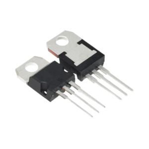
IRF3808PBF Infineon IRF3808PBF N-Channel Power MOSFET (TO-220AB) 75V 140A 330W 7mΩ@10V 4V@250uA 1 N-Channel TO-220AB Single FETs, MOSFETs ROHS
- Ultra-low conduction loss: RDS(on) 5.9 mΩ typ., 7 mΩ max @ VGS = 10 V, ID = 82 A.
- High current & ruggedness: ID = 140 A (Tc = 25 °C), IDM = 550 A, repetitive avalanche allowed up to Tj(max).
- High-temperature operation: qualified for 175 °C junction temperature with low RθJC = 0.45 °C/W for efficient heat flow.
Infineon IRF3808PBF Single FETs, MOSFETs
Specifications
(Key electrical characteristics at TJ = 25 °C unless noted; see datasheet page 2 for test conditions and full notes.
| Parameter | Value |
|---|---|
| Category | Discrete Semiconductors / FETs, MOSFETs / Single |
| Manufacturer | Infineon (International Rectifier) |
| Technology / Type | N-Channel HEXFET® Power MOSFET |
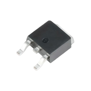
| Package | TO-220AB, through-hole (1-G, 2-D, 3-S; tab = D) |
| Drain-to-Source Voltage (VDSS) | 75 V |
| Continuous Drain Current (ID, Tc = 25 °C) | 140 A (VGS = 10 V) |
| Continuous Drain Current (ID, Tc = 100 °C) | 97 A (VGS = 10 V) |
| Pulsed Drain Current (IDM) | 550 A |
| Power Dissipation (PD, Tc = 25 °C) | 330 W; linear derating 2.2 W/°C |
| Gate-to-Source Voltage | ±20 V (max) |
| Drain-to-Source On-Resistance RDS(on) | 5.9 mΩ typ., 7.0 mΩ max @ VGS = 10 V, ID = 82 A |
| Gate Threshold Voltage VGS(th) | 2.0 – 4.0 V @ ID = 250 µA |
| Forward Transconductance (gfs) | 100 S typ. @ ID = 82 A |
| Gate Charge (Qg) | 150 nC typ., 220 nC max @ VGS = 10 V, VDS = 60 V, ID = 82 A |
| Gate-to-Source Charge (Qgs) | 52 nC typ. |
| Gate-to-Drain (“Miller”) Charge (Qgd) | 50 nC typ. |
| Turn-On Delay / Rise Time | td(on) ≈ 15 ns typ.; tr ≈ 140 ns typ. (test conditions per datasheet) |
| Turn-Off Delay / Fall Time | td(off) ≈ 120 ns typ.; tf ≈ 120 ns typ. |
| Input Capacitance (Ciss) | ~5310 pF @ VGS = 0 V, f = 1 MHz |
| Reverse Transfer Capacitance (Crss) | ~130 pF @ VGS = 0 V, VDS sweep, f = 1 MHz |
| Output Capacitance (Coss) | Condition-dependent; e.g., 890 pF @ VDS = 25 V; also characterized at 10 V and 60 V (see table) |
| Body Diode Continuous / Pulsed Current (Is / Ism) | 140 A / 550 A (integral fast body diode) |
| Body Diode Forward Voltage (VSD) | ~1.3 V typ. @ ID = 82 A |
| Reverse-Recovery Time (trr) | 93 ns typ., 140 ns max @ di/dt = 100 A/µs |
| Reverse-Recovery Charge (Qrr) | 340 nC typ., 510 nC max @ di/dt = 100 A/µs |
| Single-Pulse Avalanche Energy (EAS) | 430 mJ (starting TJ = 25 °C; L = 0.13 mH) |
| Avalanche Current (IAR) | 82 A (see figures for repetitive avalanche guidance) |
| dv/dt Ruggedness (diode recovery) | 5.5 V/ns (peak) |
| Thermal Resistance, Junction-to-Case (RθJC) | 0.45 °C/W max |
| Thermal Resistance, Case-to-Sink (RθCS) | 0.50 °C/W typ. (flat, greased) |
| Thermal Resistance, Junction-to-Ambient (RθJA) | ~62 °C/W (free air) |
| Operating Junction Temperature (TJ) | −55 °C to +175 °C; storage −55 °C to +175 °C |
| Qualification | Designed and qualified for Automotive (AEC-Q101) |
| Soldering / Mounting | 300 °C for 10 s (1.6 mm from case); mounting torque 1.1 N·m (6-32/M3) |
Notes on capacitances: the datasheet characterizes Ciss/Coss/Crss across operating voltages; use the condition that matches your topology (e.g., Coss @ 25 V for 12–24 V bus, or the tabulated “effective Coss” for resonant designs). See the full table and graphs on page 2.
Applications
Automotive power stages (12 V/24 V/48 V): The IRF3808PBF was designed with automotive use in mind and is qualified accordingly. Its low RDS(on) and high current rating reduce conduction losses in high-side or low-side positions of e-pump controllers, fans, EPS/EPB, seat/door/lift systems, and 48 V mild-hybrid auxiliaries. The robust avalanche rating and 175 °C capability provide margin for load dumps and under-hood thermals.
Motor drives & motion control: As a low-loss switch in BLDC/PMSM inverters, H-bridges, and brushed DC controllers, the device’s 5.9–7 mΩ RDS(on) helps maximize torque per watt while keeping device temperatures in check. Short trr and moderate Qg aid switching efficiency at typical 10–30 kHz PWM frequencies.
High-current DC-DC and server/telecom rails: In synchronous buck and multiphase step-down stages operating from 12 V or 24 V, the device can serve as a low-side MOSFET where conduction loss dominates, or as a rugged high-side for converters with higher transient stresses. The combination of low RDS(on), low RθJC, and well-behaved capacitances improves overall η, especially at high load.
Battery protection, OR-ing, and hot-swap: The HEXFET structure handles high surge currents, and the body diode plus low RDS(on) favor active OR-ing and pack protection MOSFET arrays in energy storage and UPS modules. Avalanche and dv/dt ratings add protection during fault events.
General power switching: Suitable for high-current solenoids, heaters, and resistive/inductive loads in factory automation, robotics, and power distribution at ≤ 75 V.
Design tips & selection guidance (practical notes)
-
Gate drive: The performance numbers (RDS(on), Qg) are specified at VGS = 10 V. For logic-level drive systems, ensure the driver can deliver ≥ 10 V (or validate RDS(on) at your actual VGS). A strong gate driver with a few amps peak helps manage switching loss given Qg ≈ 150–220 nC.
-
Thermal path: With RθJC of 0.45 °C/W and PD up to 330 W at Tc = 25 °C, the device rewards good heatsinking. Keep the case-to-sink interface low in impedance (RθCS ≈ 0.5 °C/W greased, per datasheet) and observe torque specs to maintain flatness and pressure.
-
Diode behavior: For synchronous rectifier roles, the body diode’s trr/Qrr are moderate; dead-time optimization and snubbing can further reduce losses and EMI. See page 2 parameters and the diode recovery dv/dt rating of 5.5 V/ns.
-
Ruggedness: The device allows repetitive avalanche up to Tj(max) with guidance in Figures 12–16; verify your inductive energy and current fall within recommended limits. (Referenced in the rating notes on pages 1–2.)
Why this device? If you are building high-current 12–48 V systems and need a proven, automotive-grade MOSFET with ample current headroom, low conduction loss, and solid thermal performance—without moving to exotic packaging—the IRF3808PBF is a reliable, widely supported choice. Its TO-220AB form factor eases prototyping and serviceability while still delivering excellent efficiency and robustness under real-world stress.
Package & marking reference: The datasheet (page 9) shows the JEDEC TO-220AB outline and part-marking details; lead-free versions are denoted with “PbF” and a “P” in the assembly line position.
Note on conflicting third-party data: You may see web summaries incorrectly label IRF3808PBF as a P-channel device or cite lower current ratings. The official datasheet clearly specifies an N-channel device with ID = 140 A (Tc = 25 °C) and RDS(on) ≤ 7 mΩ @ 10 V. Always design to the datasheet.
Specification: Infineon IRF3808PBF N-Channel Power MOSFET (TO-220AB) 75V 140A 330W 7mΩ@10V 4V@250uA 1 N-Channel TO-220AB Single FETs, MOSFETs ROHS
|
User Reviews
Only logged in customers who have purchased this product may leave a review.
Related Products


There are no reviews yet.