
XMSM0C1104S8YCJR XMSM0C1104S8YCJR – Tiny DSBGA-8 prototype-only MCU with full MSPM0C1104 feature set
-
DSBGA-8 footprint for the smallest prototypes and z-height budgets.
-
Full MSPM0C1104 feature set (24-MHz M0+, 12-bit ADC, UART/I²C/SPI) in a minuscule package.
-
Explicit X-device status to de-risk production—prototype now, change package later.
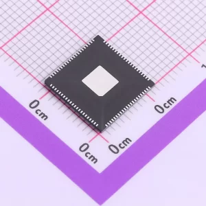
Texas Instruments XMSM0C1104S8YCJR Microcontroller (DSBGA-8, Experimental) Overview
XMSM0C1104S8YCJR is an X-prefix experimental orderable for the MSPM0C1104 in an 8-ball DSBGA (YCJ). Per TI’s nomenclature, “X” devices are developmental and not intended for production; specifications and availability can change, and long-term quality data may be incomplete. Use this device for internal evaluation, proof-of-concepts, and form-factor studies where absolute minimum area is required.
Functionally, target the familiar 24-MHz Arm® Cortex®-M0+, 16KB Flash / 1KB SRAM, 12-bit ADC up to 1.5 Msps, UART/I²C (FM+)/SPI, timers/PWM, and ultra-low-power modes—but plan for tight pin budgeting and DSBGA-specific assembly/inspection constraints. When you’re ready to harden the design, migrate to a production package (e.g., SOT-16, VSSOP-20, WQFN-20) with near-drop-in firmware reuse.
What’s different about the DSBGA X-device
-
Prototype-only status: best for size exploration and early risk retirement—do not baseline a production BOM on this orderable.
-
Board space minimalism: DSBGA-8 enables the smallest MSPM0C1104 footprint, suitable for stickers, micro-tags, and stacked flex modules.
-
Assembly realities: requires fine-pitch processes, X-ray inspection, and often underfill for robustness; hand rework is impractical.
-
Pin economy: 8 balls demand careful muxing—choose one primary serial bus, plan ADC channels early, and preserve a debug route during bring-up.
Specifications
| Parameter | Value |
|---|---|
| Status | Experimental X device (prototype only; non-production) |
| Core | Arm Cortex-M0+ @ up to 24 MHz (internal oscillator) |
| Memory | 16KB Flash, 1KB SRAM |
| ADC | 12-bit, up to 1.5 Msps; internal/external reference options |
| Comms | UART / I²C (FM+) / SPI; DMA for ADC |
| Low-power | RUN ~87 µA/MHz; STANDBY ~5 µA; SHDN ~200 nA |
| Package | 8-ball DSBGA (YCJ) – orderable XMS…S8YCJR |
| Base Product Number | MSPM0C1104 |
Applications (prototype-stage only)
-
Proof-of-concepts & lab demos where board area is the gating constraint.
-
Wearable/medical research boards (non-production) needing ultra-low z-height and tiny footprints.
-
Sensor stickers & experimental tags—beacons, event detectors, disposable trials.
-
Form-factor studies before committing to SOT/WQFN footprint decisions.
Three quick features
-
DSBGA-8 footprint for the smallest prototypes and z-height budgets.
-
Full MSPM0C1104 feature set (24-MHz M0+, 12-bit ADC, UART/I²C/SPI) in a minuscule package.
-
Explicit X-device status to de-risk production—prototype now, change package later.
DSBGA layout & assembly guidance (lab-centric)
-
Fan-out strategy: expect via-in-pad (filled/capped) or microvias; keep escape routes short and symmetric to reduce skew on SPI/clock lines.
-
Solder mask & stencil: use solder-mask-defined pads with a thin stencil (e.g., 3–4 mil) to control paste volume and avoid bridging/ball float.
-
Underfill & reliability: consider capillary underfill for shock/vibration; validate with thermal cycling if you intend to move on-body or mobile.
-
Inspection: plan for X-ray (AOI can’t see under DSBGA); build golden samples to calibrate voiding acceptance.
-
Rework: assume non-reworkable; design a castellated or mezzanine adapter for iterative firmware/hardware changes.
-
ESD & handling: adopt strict ESD controls; DSBGA dies are less forgiving of mishandling than leaded packages.
Bring-up workflow (minimize risk)
-
Pin budget first: choose I²C as the primary sensor backbone in most cases; reserve a route for UART debug during early tests.
-
Clock & power early: verify internal SYSOSC accuracy against protocol needs; instrument run vs. sleep current early to hit battery goals.
-
ADC hygiene: short, shielded analog routes; use internal 2.5 V VREF for wider span or 1.4 V for low-range precision.
-
Firmware portability: keep HAL/driver layers package-agnostic so you can migrate to SOT-16 / VSSOP-20 / WQFN-20 with minimal code edits.
Migration path to production (critical)
-
Nearest production substitutes:
-
SOT-16 (SDYYR): balanced I/O in a leaded, inspection-friendly body.
-
VSSOP-20 (SDGS20R): compact, richer I/O without going leadless.
-
WQFN-20 (SRUKR): lowest z-height with exposed pad for thermal/ground integrity.
-
-
Pin map discipline: maintain a logical pin/feature map now to ease remap later; avoid hard-coding ball names in app code.
-
Validation gates: only promote to NPI after you’ve re-built the design on a production package and re-run EMC, power, and lifetime tests.
Risk & readiness checklist (use before any wider pilot)
-
✅ Confirm X-device status is acceptable to your program and purchasing.
-
✅ Verify assembly house can handle DSBGA with X-ray and (if needed) underfill.
-
✅ Lock debug access (pads/fixture) before panelization.
-
✅ Document a package-migration plan with alternate orderables and re-layout effort.
-
✅ Capture current, timing, and ADC performance baselines to compare after migration.
Summary
XMSM0C1104S8YCJR is your ultra-miniature, lab-only path to exploring MSPM0C1104 in the tightest possible footprint. Use it to de-risk size, routing, and power on early prototypes—then migrate to a production-qualified package for release. This approach preserves your firmware investment while avoiding the pitfalls of locking a product to an experimental orderable.
Specification: XMSM0C1104S8YCJR – Tiny DSBGA-8 prototype-only MCU with full MSPM0C1104 feature set
|
Related Products