
MSPM0C1104SRUKR MSPM0C1104SRUKR – Low-profile, high-I/O 24-MHz MCU in WQFN-20 with exposed pad
-
Leadless WQFN + exposed pad for solid grounding and heat spreading.
-
Family low-power + fast wake to balance responsiveness and battery life.
-
12-bit ADC to 1.5 Msps for rapid, repeatable sampling in small form factors.
Texas Instruments MSPM0C1104SRUKR Microcontroller (WQFN-20) Overview
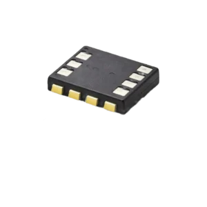
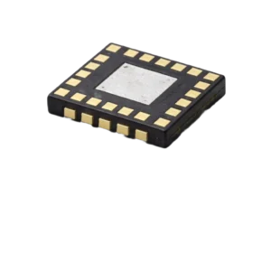
MSPM0C1104SRUKR packages TI’s MSPM0C110x mixed-signal feature set in a 20-pin WQFN (RUK) with an exposed thermal/ground pad, delivering maximum I/O density in the lowest z-height of the family. Compared with leaded SOT/VSSOP, WQFN minimizes loop inductance, improves ground impedance for the ADC and timers, and enables tighter, denser layouts—ideal for slim modules, stacked boards, and space-constrained enclosures.
You still get the core family features: 24-MHz Arm® Cortex®-M0+, 16KB Flash / 1KB SRAM, 12-bit ADC up to 1.5 Msps (ENOB >10 bits typical), UART / I²C (FM+) / SPI, and ultra-low-power modes with fast wake. The exposed pad gives you a robust thermal and EMI return plane, letting this tiny MCU punch above its size in mixed-signal performance.
Highlights (why choose WQFN-20)
-
Ultra-low profile, high I/O: smallest z-height with broad pin access for multi-sensor, multi-PWM, or dual-bus designs.
-
Exposed-pad advantage: low-impedance ground for ADC accuracy, PWM edge control, and EMI containment.
-
Cleaner high-speed routing: short, symmetric traces benefit SPI up to ≤12 Mbps and time-critical control loops.
-
Dense, manufacturable layouts: fine-pitch, leadless footprint enables compact modules and stacked daughtercards.
-
Family consistency: same silicon and software as other MSPM0C1104 packages; migrate by I/O needs, not by codebase.
Specifications
| Parameter | Value |
|---|---|
| Core | Arm Cortex-M0+ @ 24 MHz (SYSOSC ±~1.2% with FCL) |
| Memory | 16KB Flash / 1KB SRAM |
| ADC | 12-bit up to 1.5 Msps; internal 1.4 V / 2.5 V VREF; ENOB >10 bits typical |
| Interfaces | UART / I²C (FM+) / SPI ≤12 Mbps; DMA for ADC |
| Timers | 1 advanced + 2 general-purpose (up to 14 PWM total at family level) |
| GPIO | Up to 18; two 5-V tolerant open-drain pins (package-dependent) |
| Power | 1.62–3.6 V; RUN ~87 µA/MHz; STANDBY ~5 µA; SHDN ~200 nA |
| Package | 20-pin WQFN (RUK) with exposed pad – orderable SRUKR |
| Base Product Number | MSPM0C1104 |
Applications
-
Space-limited control boards with strict z-height — thermostat PCBs, sensor tiles, stacked mezzanines.
-
Sensor hubs & multi-PWM lighting engines — stable ADC ground, tidy PWM routing for flicker-free control.
-
Smart modules & embedded nodes — radio or transceiver companion MCU with low EMI footprint.
-
Compact industrial I/O slices — dense GPIO, quick SPI/I²C busing, and robust thermal return in tight bays.
Three quick features
-
Leadless WQFN + exposed pad for solid grounding and heat spreading.
-
Family low-power + fast wake to balance responsiveness and battery life.
-
12-bit ADC to 1.5 Msps for rapid, repeatable sampling in small form factors.
Layout & assembly guidance (WQFN-specific)
-
Pad and plane strategy: treat the exposed pad as primary GND; stitch with a via array into the ground plane directly under the device to reduce return impedance for ADC and timers.
-
Stencil & paste: use a window-pane stencil on the exposed pad (≈50–70% paste coverage) to avoid float/voids; perimeter pads should be solder-mask-defined for consistent fillets.
-
Via-in-pad: if needed for density, use filled/capped microvias on the exposed pad; otherwise, tent vias to control wicking.
-
Signal integrity: fan-out SPI/clock lines on the shortest escape layer; keep them away from ADC inputs and VREF routes.
-
Thermal: tie heat sources (drivers/LED FETs) into the same ground island so the exposed pad acts as a shared spreader, then isolate analog grounds locally before a single-point tie to the pad.
Mixed-signal partitioning (do more in less space)
-
ADC/VREF hygiene: dedicate a quiet polygon around analog pins; keep high-di/dt PWM edges and chip-selects off that boundary.
-
PWM timing: use the advanced timer for center-aligned PWM or higher resolution dimming; place gate drivers adjacent to reduce loop area.
-
Reference options: select 1.4 V VREF for low-range, low-noise sensors; 2.5 V for wider span without external references.
Power & firmware strategy
-
Event-driven firmware: idle in STANDBY, wake from GPIO/RTC/ADC thresholds; return to sleep quickly.
-
Shelf mode: enable SHDN (~200 nA) for storage/shipping.
-
Throughput budgeting: ~87 µA/MHz → ≈2.1 mA @ 24 MHz baseline; gate clocks and use DMA for ADC bursts to shorten active windows.
How it differs from your other package choices
-
vs. SOT-16 (SDYYR): lower z-height and better ground impedance for ADC/EMI; requires tighter assembly control (no gull-wing leads).
-
vs. VSSOP-20 (SDGS20R): smaller profile and improved return paths; VSSOP is easier to AOI/rework but taller.
-
vs. 8-pin SOT/WSON (SDDFR/SDSGR): far more I/O and cleaner partitioning; WSON is also low profile, but WQFN-20 offers significantly richer pinout.
Summary
If your design is height-constrained but needs real I/O breadth, clean ADC performance, and efficient thermal/EMI returns, MSPM0C1104SRUKR (WQFN-20) is the sweet spot. You get the smallest profile with an exposed pad for grounding and heat—exactly what dense control boards, sensor hubs, and sleek smart modules need.
Specification: MSPM0C1104SRUKR – Low-profile, high-I/O 24-MHz MCU in WQFN-20 with exposed pad
|
Related Products