
Semiconductor-ICs
Showing 1–30 of 172 results

- One-Time Programmable (OTP): Fuse-link technology locks resistance permanently after final adjustment.
- Wide Resistance Range: 100kΩ end-to-end resistance with ±30% tolerance.
- I2C Interface: Simple 2-wire control with selectable address (AD0 pin) for multi-device configurations.
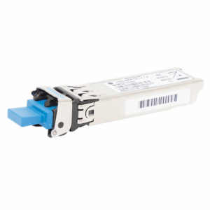
- 10km SMF Reach – 1310nm wavelength over single-mode LC fiber.
- TAA & MSA Compliant – Guaranteed 100% OEM compatibility.
- DOM Support – Real-time monitoring of power/temperature/LOS.
- Fixed 3.3V Output – Tight tolerance (±1.5%) for precision circuits.
- Low Dropout Voltage – Only 1.2V typical at 1A load.
- High PSRR (75dB) – Excellent ripple rejection for noise-sensitive applications.
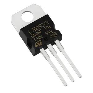
- Fixed 5V Output – Tight tolerance (±1.5%) for precision applications.
- Low Dropout Voltage – Only 1.2V typical at 1A load.
- Thermal Protection – Auto-shutdown at 150°C to prevent damage.
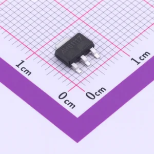
- Wide Voltage Range (3V–18V) – Supports high-voltage logic applications
- Low Input Current (100nA at 25°C) – Minimizes power consumption
- Balanced Symmetrical Outputs – Ensures uniform switching times (30ns typical)
-
DSBGA-8 footprint for the smallest prototypes and z-height budgets.
-
Full MSPM0C1104 feature set (24-MHz M0+, 12-bit ADC, UART/I²C/SPI) in a minuscule package.
-
Explicit X-device status to de-risk production—prototype now, change package later.
- Tri-radio on one chip: Dual-band Wi-Fi 6 + BLE 5 + IEEE 802.15.4 for Thread/Zigbee in a single, compact MCU.
- Security built-in: Secure boot, XTS-AES memory encryption, HMAC, RSA/ECC/ECDSA, TRNG, APM & PMP hardening—ready for zero-trust IoT.
- Designed for battery life: LP RISC-V core, deep-sleep with LP SRAM retention, Wi-Fi TWT, and fine-grained PMU control.
- Tri-radio in one chip: Wi-Fi 6 + Bluetooth LE 5.3 + 802.15.4 (Zigbee/Thread) with built-in coexistence on a single antenna.
- Secure by design: Secure boot, XTS-AES flash encryption, digital signature, RSA/ECC, and HMAC in hardware.
- Ultra-low power: Deep-sleep around 7 µA with LP-SRAM retention and Target Wake Time to extend battery life.
- Low power without compromises – Deep-sleep around 7 µA with LP memory retention, fast wakeup, and flexible PMU states. ETM and GDMA enable peripheral-driven data paths so your CPU can nap.
- Security you can ship – Secure Boot, flash encryption, and a full hardware crypto suite (AES/SHA/RSA/ECC/ECDSA/HMAC), plus a power-glitch detector and true RNG, help protect firmware/IP and elevate trust.
- Radio versatility – Bluetooth LE 5.3 with 2 M and Coded PHY for either speed or range, plus 802.15.4 for Thread/Zigbee/Matter—covering the majority of modern IoT transports with one tiny chip.
-
Dual-core HP RISC-V up to 360 MHz + LP RISC-V up to 40 MHz for always-on tasks.
-
Rich vision & video engine: JPEG codec, ISP (1080p), PPA (scale/rotate/blend), H.264 encoder (1080p@30 fps).
-
Comprehensive security: Secure Boot, XTS-AES flash/PSRAM encryption, TRNG, RSA/ECDSA/HMAC/SHA accelerators, and access-permission management.
- USB device/host ready: Full-speed USB OTG with on-chip PHY streamlines accessories and field update paths.
- ULP always-on sensing: A dedicated ULP coprocessor handles RTC GPIO/ADC/touch while the main CPU sleeps.
- Hardened security chain: Secure boot + flash encryption + hardware AES/SHA/RSA and true RNG.
-
USB all the things: Native USB 2.0 Full-Speed OTG plus a built-in USB-Serial/JTAG device for programming, logging, and on-chip debug with minimal parts.
-
Vision & UI ready: Parallel LCD (8–16-bit RGB/I8080/6800) and DVP camera interfaces up to 40 MHz, with YUV/RGB conversions for low-cost displays and sensors.
-
Hardened by design: Secure Boot, Flash Encryption, AES-128/256, SHA-2, RSA up to 4096-bit, HMAC, Digital Signature, and TRNG for modern, production-grade security.
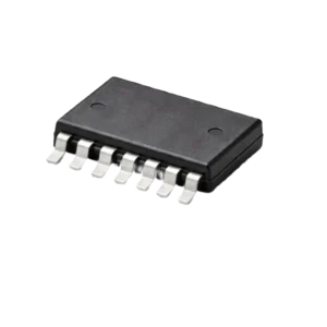
- Stable 5V / 1.5A output
- Excellent protection (thermal, short circuit)
- High PSRR and low noise performance
1111